CLAWS
What is a wide-bandgap semiconductor?
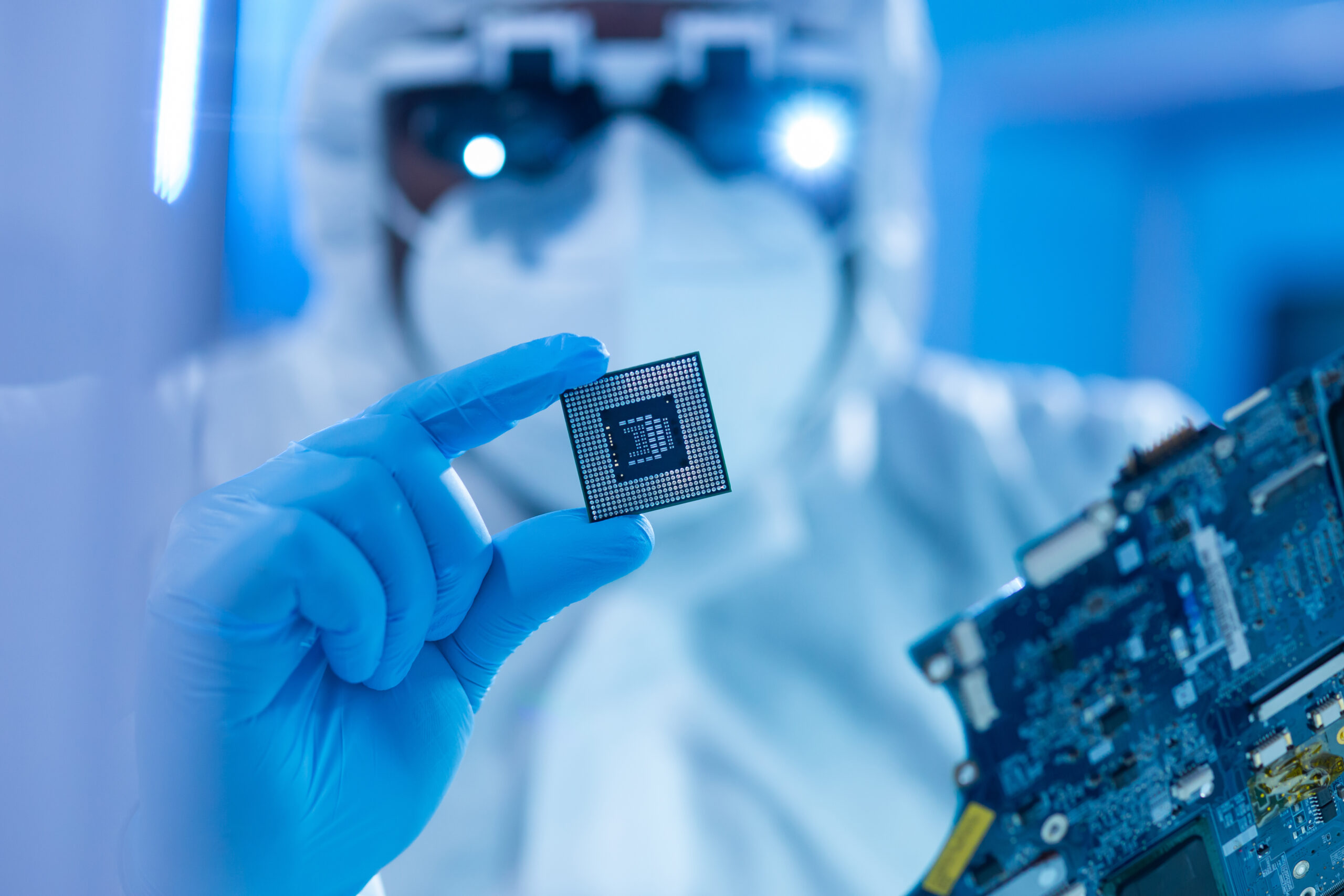
Wide-bandgap semiconductors like Silicon Carbide, Gallium Nitride enable electronic
devices to operate at much higher voltages, frequencies, and temperatures and more
efficiently than silicon. This is great for DoW and civilian applications where Size,
Weight, and Power (SWaP)matter, allowing more electronics on airplanes and satellites, electric vehicles that go further on a battery charge, more powerful and accurate Radars, and faster communication systems. Emerging ultra-wide bandgap semiconductors like Diamond and Gallium Oxide can operate at even higher voltages and may be part of shipboard systems and future electric power grids.
What is the Microelectronic Commons?
The Microelectronics Commons is a national network of prototyping innovation hubs. The Microelectronics Commons is creating a direct pathway to reduce the country’s reliance on foreign microelectronics and safeguard the nation from supply chain risks.
The Commercial Leap Ahead for Wide bandgap Semiconductors (CLAWS) Hub is focused on advancing technologies for DoW that have dual-use solutions for civilians.
What does Commercial Leap Ahead mean?
“Leap ahead” technologies are highly innovative technologies that have the potential to provide significant advantages, particularly against near-peer adversaries, and are associated with “war-winning” capabilities.
“Commercial leap ahead” refers to the adoption of these cutting-edge technologies by
commercial industries.
CLAWS Hub Featured on ABC11
Federal officials announce semiconductor funding award.
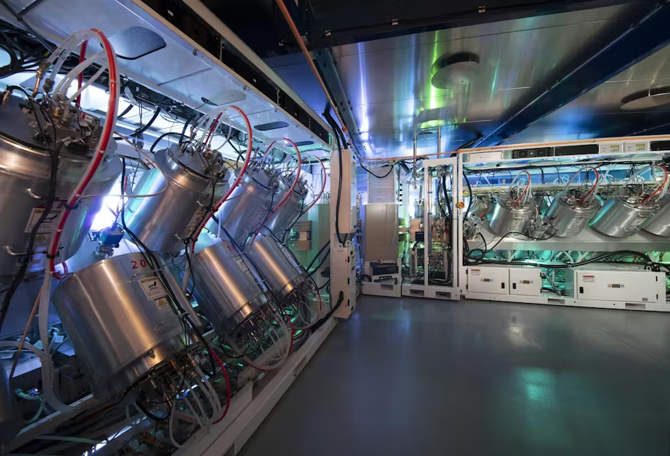
What is a research foundry?
In traditional foundries very rigid sets of rules are used to ensure that the same identical chip can be made time after time. These rules are implemented in a Process Design Kit (PDK) and if your idea or design doesn’t follow the PDK, it becomes very difficult often becoming economically not feasible to implement in that foundry. This lengthens R&D cycles and can stifle innovation.
CLAWS employs a new Research Foundry approach to accelerate innovation and development wherein baseline processes, process blocks, and device flows are integrated to work together and maintained under statistical process control (SPC) to ensure high quality and reproducibility. However, unlike a traditional rigid foundry model, the Research Foundry enables modifying baseline processes, process blocks, and device designs. It leverages, where possible, known characterized, and maintained baseline capabilities, allowing designers and engineers to change selected parts of the process to implement new ideas. As a result, the Research Foundry enables more efficient research, focused innovation, the attainment of a higher level of integration.
Furthermore, the Research Foundry can engage a wider community of researchers who can utilize the new capability with less materials, process, device, and/or circuit knowledge than typical for semiconductors at lower technology readiness levels.
CLAWS implements the increased flexibility of the Research Foundry via the new concept of Research Development Kits (RDKs), which will provide a modular approach to process blocks and process flows, and, when coupled with hub developments in Electronic Design Automation (EDA) tools, will allow DOW users to access and innovate WBG and UWB technologies.
Learn more about our workforce development efforts
Latest News
Read more
USAF Veteran Credits CLAWS-funded Credentialing Program
Axcelis, GE Aerospace team on silicon carbide power device development
Kyma Technologies and Novel Crystal Technology Announce Strategic Collaboration for Next-Generation Power Electronics